
Driven by continuous iteration toward higher computing‑density architectures including NVIDIA Vera Rubin, AMD Helio, Google TPU and AWS Trainium platforms, the total PCB area required per rack keeps expanding from the rack‑platform perspective.
Take the NVIDIA Vera Rubin platform as an example. It adopts a Midplane central interconnect board. The Rubin Ultra (Kyber) variant further employs a 78‑layer orthogonal backplane to replace thousands of NVLink copper cables. According to SemiAnalysis estimates, the total area of high‑end high‑speed PCBs within the Rubin NVL72 rack rises approximately 2.3‑fold compared with the GB300.
In terms of CCL grades and PCB manufacturing processes, CCL specifications are shifting from grade M7 toward dominant M8 with gradual penetration of M9. PCBs are evolving toward high‑layer‑count structures, oversized dimensions, and stringent controls over signal integrity, impedance and insertion loss.
Comparing NVIDIA Vera Rubin VR200 against its predecessor GB300:
GB300: Compute boards adopt 22‑layer, 5‑stage HDI with M7‑grade materials; switch boards use 24‑layer M8 materials, together with standard E‑glass fabric and HVLP3 copper foil.
Vera Rubin VR200: Compute boards feature 26‑layer, 6‑stage HDI with M8‑grade materials; NVSwitch switch boards adopt 32‑layer M8 materials. The 44‑layer Midplane mid‑backplane and CPX inference module boards introduce M9‑grade substrates plus Q‑glass fabric, alongside HVLP4/HVLP5 ultra‑low‑profile copper foil. These deliver low Dk and low Df properties to accommodate long‑distance backplane routing for 224G SerDes (NVLink6).
Per Morgan Stanley’s report AI Infrastructure: Materials Supercycle, global CCL market growth is primarily fueled by AI data‑center deployments. AI data centers will contribute 90 % of total CCL market incremental demand, and by 2030 this segment will account for nearly two‑thirds of overall global CCL consumption. Breaking down incremental demand, 84 % of AI‑related CCL volume growth stems from specification upgrades and higher per‑rack material value, while merely 16 % originates from rising server unit shipments.
Investment in AI computing infrastructure directly stimulates demand for copper‑clad laminates (CCL), HVLP high‑end copper foil and electronic glass fabric. Unlike cyclical swings for conventional bulk commodities, the current tightness represents structural shortage caused by surging AI‑driven demand lagged by constrained high‑end‑material supply. Qualified supplier pools for M7, M8 and M9‑grade CCL and matching copper foil shrink progressively amid rising certification barriers. Constrained by low production yields, effective supply of high‑end CCL will remain tight through the end of 2027.
Against this backdrop, capacity diversion exerted by high‑grade substrates upon generic FR‑4 merits sustained attention. This squeeze is not achieved through simple production‑line conversion; it represents dual‑sided pressure across supply and demand. On one hand, high‑end CCL delivers materially better profit margins than commodity FR‑4. Leading manufacturers dynamically allocate core‑process resources such as hot‑pressing and compounding, prioritizing production scheduling for high‑margin high‑speed‑substrate orders.
On the other hand, upstream inputs including HVLP ultra‑low‑profile copper foil, specialty electronic glass fabrics and specialized resins for high‑end substrates are pre‑emptively secured, indirectly diverting raw‑material supply for standard FR‑4. Meanwhile, near‑term new industry capacity is overwhelmingly targeted at high‑end high‑speed substrates, with minimal investment in commodity FR‑4, further aggravating structural imbalance.
Generic FR‑4 may stay in a prolonged scenario of “capacity diversion and raw‑material competition”. Supply‑demand and pricing divergence between high‑performance and general‑purpose substrates is expected to persist through the first half of 2027.
Electronic yarn is manufactured from mineral feedstocks including pyrophyllite and quartz sand. Raw materials are melted at high temperature to produce molten glass, which is drawn into glass fiber through platinum‑rhodium alloy bushings. Temperature, drawing speed and tension must be tightly controlled during fiber drawing to guarantee uniform fiber diameter and mechanical strength.

Source:IQSdirectory.com
Electronic yarn typically features diameters ≤ 9 μm, and its manufacturing accounts for 50 %‑60 % of electronic‑fabric production costs. Production of ultra‑fine yarn (< 4 μm diameter) is currently monopolized by a small number of firms such as Nittobo and AGY of the United States, with domestic self‑sufficiency below 15 %.
Electronic yarn constitutes the upstream source of the ongoing PCB raw‑material shortage:
Stagnant growth in effective supply: Global net new electronic‑yarn capacity reached 98 kt (+6.6 %) in 2025 but fell sharply to 59 kt (+3.2 %) in 2026. Although two new tank‑furnace lines totaling 135 kt were commissioned from January to May 2026, long furnace‑baking cycles limit real supply expansion.
Low upstream willingness for capacity expansion: Electronic‑yarn tank furnaces are capital‑intensive assets requiring heavy investment and lengthy construction timelines. Once ignited, furnaces must run continuously for years before cold repair. From project initiation to full‑rate production, new glass furnaces take more than two years. Soaring prices for platinum‑rhodium alloy bushings — critical precious‑metal components for glass‑fiber drawing — further raise total capital expenditure for new furnaces.
Insufficient market inventory: Some manufacturers report “zero stock”. Quota‑based allocation is widely implemented, with most customers receiving only approximately 60 % of their requested volumes.
Woven from electronic yarn, electronic fabric acts as an essential reinforcement material for copper‑clad laminates. It provides electrical insulation, mechanical support, resin retention, and guarantees mechanical and electrical performance of laminates. As downstream requirements keep upgrading, electronic‑fabric selection grows increasingly granular. The industry classifies electronic fabrics primarily by thickness and functional characteristics.
Classification by thickness — well‑known designators such as 7628, 2116, 1080 and 106 represent fabric specifications encapsulating yarn properties, warp‑and‑weft density and areal weight:
Heavy‑weight fabrics: 7628 is typical, deployed for power boards and thick multi‑layer industrial PCBs to secure structural rigidity.
Medium‑thin fabrics: 2116 and 1080 serve mainstream conventional multi‑layer boards and entry‑level high‑speed boards, balancing impedance design and manufacturing yield.
Ultra‑thin fabrics: 106, 1035, 1067 are used for HDI high‑density interconnect boards to form thin dielectric layers.
Classification by function, where fabric variants are selected according to PCB application scenarios:
Low‑Dk / Low‑Df fabrics: Offer low dielectric constant and low dissipation factor to mitigate signal loss and boost transmission speed. Second‑generation low‑dielectric glass delivers Dk 3.8‑4.2 and Df ≤ 0.015, suitable for server high‑speed boards and base‑station RF boards. Third‑generation Q‑glass (quartz fabric) is made from high‑purity quartz fiber, mostly in ultra‑thin formats. It delivers best‑in‑class dielectric performance (Dk ≤ 3.5, Df ≤ 0.005), serving AI compute hardware, high‑capacity switches and premium semiconductor packaging substrates. Global supply remains highly concentrated and dominated by Nittobo and AGC.
Low‑CTE fabrics: Formulated and engineered for low coefficient of thermal expansion, deployed for advanced IC substrates and high‑order HDI boards.
Electronic fabrics are almost exclusively produced on air‑jet looms. Finer yarn and higher weft density demand extremely precise tension control. Fine glass yarn is brittle; minor tension fluctuations cause yarn breakage. Stable mass production requires tension accuracy at ±0.1 g‑level, heavily reliant on high‑end Toyota JAT looms.
Lower stable operating speeds reduce per‑machine throughput. If output efficiency for 7628 fabric is indexed as 100 %, 1080 fabric achieves only 70 %, while 106 fabric yields merely 30 %‑50 %.
Today’s electronic‑fabric bottleneck lies in high‑end air‑jet looms. Toyota JAT910 looms capture more than 90 % of the global installed base. Monthly loom output capacity stands at merely 120‑200 units with lead‑times of 18‑24 months; new orders are already booked out to 2029.
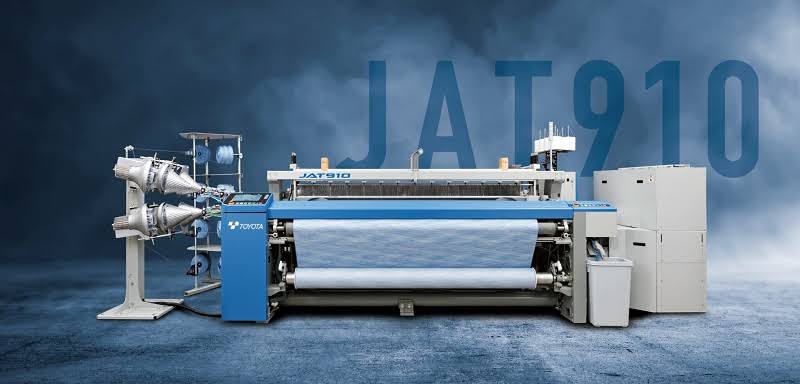
Toyota JAT910
The electronic‑fabric sector is experiencing a once‑in‑a‑decade super‑cycle, gaining further momentum. From September 2025 through October 2026, 7628 heavy‑weight fabric rose approximately 258 % cumulatively. 2116 / 1080 medium‑thin fabrics climbed 280 %‑290 %. End‑to‑end inventory across the value chain has shrunk to only 7‑10 days. Lead‑times for Low‑Dk and ultra‑thin fabrics stretch into 2027.
Copper‑clad laminates are manufactured by impregnating glass fabric with resin and laminating together with copper foil. Resins fulfill four core roles: inter‑layer adhesion, electrical insulation, CTE modulation, and tuning of dielectric constant (Dk) and dissipation factor (Df).
Low‑dielectric, low‑loss specialty resins represented by PPO (polyphenylene oxide), hydrocarbon resin, BCB (benzocyclobutene) and PTFE (polytetrafluoroethylene) define the performance ceiling of high‑end CCL.
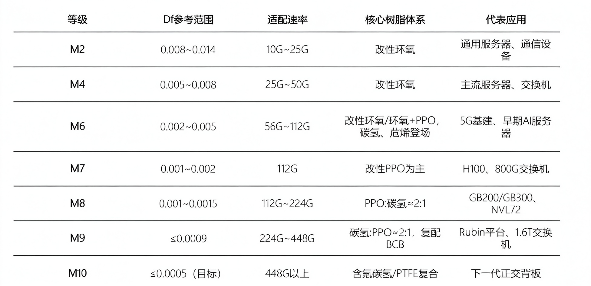
Moving from M8 toward M9 grades, the hydrocarbon‑resin mixing ratio shifts from roughly 1:2 to 2:1, bringing about a step‑jump in consumption as hydrocarbon resin evolves from auxiliary additive to primary constituent. Market demand is projected to hit 5 000‑6 000 tons by 2027. Global supply of electronic‑grade hydrocarbon resin has long been concentrated among Japanese and US producers including Asahi Kasei and Dow. The BCB market is even more concentrated, with Dow holding approximately 99 % market share. Capacity expansion cycles for these materials span 2‑3 years, leaving near‑term supply gaps difficult to close.
For PPO, SABIC was once the world’s primary sole supplier of electronic‑grade PPO, shipping around one‑thousand tons in 2022. Demand growth has far outpaced supply: global electronic‑grade‑PPO demand expanded from 1 202 tons in 2022 to 5 821 tons in 2025, representing a three‑year CAGR close to 69 %. Each AI‑server unit consumes approximately 1.60 kg of PPO — 4.7 times the volume used by conventional PCIe 5.0 servers.
High‑frequency and high‑speed performance represents the persistent upgrading theme for PCBs. Propelled by the AI‑computing boom, high‑end electronic resins have been re‑evaluated as strategic materials within the computing hardware value chain, after previously playing a comparatively under‑recognized supporting chemical role in the PCB industry.
Copper foil forms the conductive metallic layer bonded onto glass‑fabric substrates. Owing to skin‑effect behavior in high‑speed signal transmission, rougher copper‑foil surfaces increase signal scattering and insertion loss. Copper‑foil types are categorized from higher to lower matte‑side roughness (Rz): HTE, RTF and HVLP.
HTE (High‑Temperature Elongation copper foil): Rz ≈ 6‑10 μm, matte‑side rough, for generic FR‑4 and consumer‑appliance boards.
VLP (Very‑Low‑Profile copper foil): Rz ≈ 3‑5 μm, for mid‑high‑speed and mid‑range server hardware.
RTF (Reverse‑Treated Foil): Rz ≈ 2‑4 μm; the rough matte side is reversed to the bonding surface, balancing low‑loss performance and peel strength for M6/M7‑grade high‑speed boards.
HVLP (Hyper‑Very‑Low‑Profile copper foil): Rz ≈ 1.5‑3 μm, delivering best‑in‑class loss reduction. HVLP is further differentiated into generations HVLP1 through HVLP5; higher‑number grades support higher signal frequencies and are applied for M8/M9 substrates, AI servers and 224G interfaces.
The tightest supply exists for HVLP‑grade 4 and above. The HVLP4 copper‑foil market was less than USD 50 million in 2025 and is projected to reach USD 2.8 billion by 2030 at a 123 % CAGR. A 31 % supply gap is expected in 2027, easing only to 20 % in 2028. Root causes include heavy reliance on imported core surface‑treatment equipment with order backlogs extending to 2027, plus multi‑stage, long‑lead‑time qualification processes spanning copper‑foil mills, CCL manufacturers, PCB fabricators and end customers.
Carrier foil represents another constrained category. Carrier‑supported ultra‑thin copper foil (2‑5 μm functional copper) is critical for optical‑module hardware and IC substrates. Ultra‑thin copper is mechanically too fragile for direct handling and lamination. Production deposits the thin functional‑copper layer onto a 18‑35 μm thick carrier foil via a release‑treatment interlayer. After PCB lamination and drilling, the thicker carrier layer is peeled away. Booming optical‑module demand together with widespread mSAP‑process adoption creates severe supply shortages for carrier foil.
The copper‑foil industry faces rising processing fees and near‑zero‑inventory operating conditions, with leading production capacity locked under long‑term contracts. While conventional HTE copper‑foil shortages are less acute than for HVLP grades, capacity diversion toward premium variants has triggered price hikes; processing fees have doubled year‑over‑year.
Current‑day laminate suppliers enforce quota‑based allocation plus dynamic pricing rules. Each month suppliers assign fixed shipment quotas to customers; volumes exceeding monthly quotas are deferred to subsequent delivery windows. Settlement prices are based on prevailing market prices upon material arrival at customer premises; prices at order placement do not govern final invoicing.
For prototype orders: Confirm material specifications and stack‑up structures with laminate suppliers at the PCB‑design kick‑off phase and initiate procurement preparations in parallel. Leverage layout‑design cycle time to mitigate extended material‑procurement lead‑times.
For volume‑production orders: Release demand forecasts and place purchase orders two months in advance to secure allocation. For high‑frequency part‑numbers requiring recurring restocking, maintain safety‑inventory levels equivalent to 1‑2 months of consumption.
Advanced stocking cannot lock in fixed purchase prices, yet it secures material availability and mitigates the financial impact of price inflation.
When evaluating substrate‑material substitutions, thermal performance and long‑term reliability constitute primary assessment criteria, with key parameters covering Tg, Td, CTE and thermal conductivity.
For high‑speed products, impedance control sits at the core of design requirements. Substrate material changes directly alter circuit‑board electrical properties and impact signal integrity. In high‑speed applications, designers must evaluate not only dielectric constant Dk but also dissipation factor Df at target operating frequencies, and revise stack‑up configurations alongside material swaps.
UL compliance must also be verified proactively. Confirm that alternative laminates hold matching UL certifications. Note further that UL marking requirements for finished PCBs may change following substrate replacement.
Proactive DFM (Design‑for‑Manufacturability) reviews during project execution are essential for risk mitigation and cost containment. Many project‑execution difficulties stem from fragmented substrate‑material selections. Disparate designs adopting numerous distinct laminate grades complicate supplier stock preparation, extend lead‑times, and add substantial overhead for material‑swap validation and qualification maintenance.
We recommend launching DFM reviews in parallel with schematic development. Consolidate laminate‑material requirements against thermal, impedance, signal‑integrity and compliance targets. Where electrical‑performance and reliability specifications permit, rationalize and converge selected laminate grades, thicknesses and material classes to drive specification normalization.
A standardized laminate portfolio reduces material‑part diversity, streamlines supply‑chain governance, lowers overhead for subsequent re‑qualification and UL re‑assessment, mitigates engineering‑change risks at source, and accelerates transition from design to mass‑production.
PCB upstream raw‑material markets are cyclical, with lead‑times and pricing subject to constant change. Track supply‑demand shifts for copper‑clad laminates, copper foil and other upstream inputs. Adjust procurement strategies promptly once indicators signal easing lead‑times and decelerating price inflation.
 WeChat