
To pursue higher efficiency and lower power loss, power product designs are trending toward high‑voltage and high‑current configurations. Hardware engineers must pay closer attention to potential PCB failures induced by high voltage, among which inter‑layer high‑voltage failure is the most critical concern.
When voltage is applied across PCB layers, an electric field builds up between the two electrodes. In theory, the molecular structure of insulating materials (Prepreg / PP sheets) confines electrons within atoms or molecules and prevents their free migration.
Nevertheless, defects such as micro‑bubbles, impurities, or interfacial voids — which cannot be completely eliminated by practical manufacturing processes — exhibit far lower dielectric strength than the bulk material. High‑voltage failures tend to originate in these defective regions.
Stages of PCB inter‑layer high‑voltage breakdown:
Initiation of Partial Discharge: Local electric fields at defects become substantially higher than the average electric field, triggering incipient electron avalanches or partial discharges. Minor electron flow occurs from the negative electrode to the positive electrode yet remains confined within the defect.
Energy Dissipation and Heat Accumulation: As high‑energy electrons travel through the dielectric medium, inelastic collisions take place with resin molecular chains and glass fibers. Kinetic energy is converted into thermal energy, raising local temperatures.
Thermal Runaway and Carbonization: If heat generated by sustained partial discharge cannot dissipate promptly, thermal accumulation pushes local temperatures above the material’s Glass Transition Temperature (Tg) and even its Decomposition Temperature (Td). This causes epoxy resin carbonization. Carbonized by‑products (graphitic carbon) are conductive and drastically increase local current.
Breakdown Propagation: Carbonized channels keep extending until they bridge the two electrodes, forming a permanent conductive carbonized path and completing dielectric breakdown.
Multiple critical parameters govern inter‑layer high‑voltage withstand capability, namely applied voltage magnitude, dielectric thickness, material properties, as well as process‑induced defects and void control.
Voltage magnitude determines electric‑field intensity. Higher applied voltage yields greater electric‑field strength inside the dielectric, following the formula E = V/d. Stronger electric fields exert larger forces on stray free electrons within the dielectric and accelerate them to higher kinetic energy. Collisions between these energetic electrons and dielectric atoms readily dislodge bound electrons and generate additional free electrons. This chain‑reaction impact ionization produces electron avalanches.
Higher voltage accelerates electron‑avalanche formation and propagation, shortening time‑to‑breakdown and elevating failure probability. In short: higher voltage delivers stronger driving force for breakdown.
Dielectric thickness provides resistance against free‑electron penetration. Greater inter‑layer spacing means more dielectric material fills the gap. With increased separation, partial discharges struggle to evolve into full‑thickness breakdown channels. Even when local heating occurs, enormous energy is required to propagate thermal damage across the full dielectric thickness to create a conductive path.
Industry empirical rule of thumb: 1 mil dielectric thickness withstands approximately 500 V DC. Practical designs must incorporate adequate safety margins.
Per IPC‑6012F Clause 3.6.2.18.1 acceptance specifications:
This specification reflects the miniaturization trend: thinner core materials are adopted while equivalent or improved high‑voltage performance is demanded.
Clause 3.6.2.18.1 Minimum Dielectric Spacing Where minimum dielectric spacing and/or number of reinforcement layers are not specified:
- Minimum dielectric spacing shall be 90 μm [3,543 μin]; reinforcement layer count shall be selected by the supplier for designs first released on or before December 31, 2023.
Minimum dielectric spacing shall be 65 μm [2,560 μin]; reinforcement layer count shall be selected by the supplier for designs first released on or after January 1, 2024.
When nominal dielectric spacing shown on drawings is less than 90 μm [3,543 μin], the minimum dielectric spacing shall be 25 μm [984 μin], with reinforcement layer count at supplier discretion. (Cores with nominal dielectric spacing of 25 μm [984 μin] or below are excluded from this requirement.)
Note: Low‑profile copper foil shall be used for dielectrics thinner than 90 μm [3,543 μin]. Products with transmission‑line impedance requirements may define special requirements and measurement methods in procurement documentation.
Excerpted from IPC‑6012 Clause 3.6.2.18.1.
Copper‑foil type is another practical PCB‑design consideration. High‑Temperature Elongation (HTE) copper foil is widely used in general‑purpose products, with its rough side facing inward toward the dielectric and smooth side outward. For thin dielectrics (e.g., 3 mil, 4 mil), copper peaks on the rough side intrude into prepreg and effectively reduce net dielectric thickness. For thin‑core stack‑ups, Reverse‑Treated Foil (RTF) is selected by some engineers to mitigate thickness reduction caused by copper peaks.
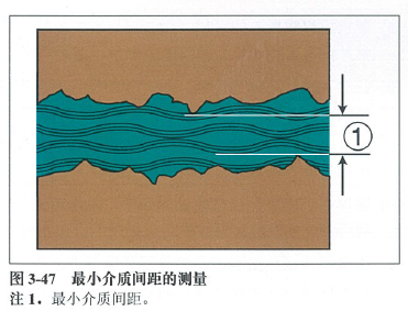
According to Figure 3‑47 within IPC‑6012F Clause 3.6.2.18, dielectric thickness is defined as the minimum distance between opposing copper peaks.
Dielectric media consist primarily of epoxy resin and glass fabric, and formulations differ among laminate suppliers. Dielectric‑withstand performance varies by material grade. Manufacturers’ datasheets provide Dielectric Strength (Electric Strength) values for material comparison.
Example parameters for RO4350B:
Multi‑ply glass‑fabric stack‑up configurations are frequently implemented during stack‑up design to boost high‑voltage endurance.
Beyond dielectric strength, the Comparative Tracking Index (CTI) and Glass‑Transition Temperature (Tg) are important for high‑voltage hardware design.
CTI characterizes resistance against surface tracking and breakdown under high‑voltage and contaminated environmental conditions. Higher CTI denotes superior resistance against conductive carbonized tracking paths under humid and polluted service conditions.
Tg represents the glass‑transition temperature. Materials with higher Tg deliver superior high‑temperature dimensional stability and reduced risks of inter‑layer delamination and micro‑cracking. Delamination compromises dielectric integrity and creates new failure‑prone defect pathways; accordingly, elevated Tg helps preserve original high‑voltage‑withstand performance.
High‑voltage PCB design requires comprehensive evaluation of applied voltage, dielectric thickness, material properties (dielectric strength, CTI, Tg), copper‑foil selection, and process void‑and‑defect mitigation. Compliance with relevant design standards and test specifications is essential to guarantee long‑term operational reliability.
 WeChat